Download
1 / 17
470 likes | 1.14k Views
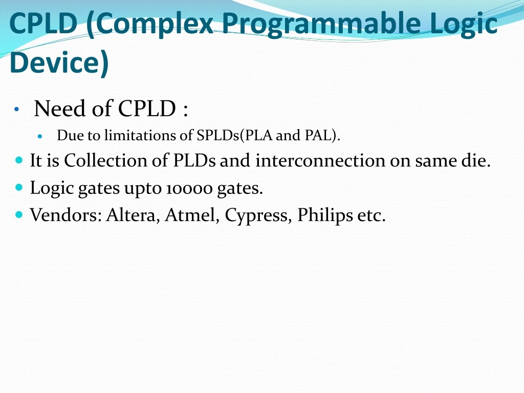
CPLD (Complex Programmable Logic Device). Need of CPLD : Due to limitations of SPLDs(PLA and PAL). It is Collection of PLDs and interconnection on same die. Logic gates upto 10000 gates. Vendors: Altera, Atmel, Cypress, Philips etc. Structural Block Diagram of CPLD. Programmablen I/O blocks.

E N D
CPLD (Complex Programmable Logic Device) • Need of CPLD : • Due to limitations of SPLDs(PLA and PAL). • It is Collection of PLDs and interconnection on same die. • Logic gates upto 10000 gates. • Vendors: Altera, Atmel, Cypress, Philips etc.
Structural Block Diagram of CPLD • Programmablen I/O blocks PLD PLD PLD Programmable Interconnect PLD PLD PLD
Macrocell: • Consists: • AND-OR configuration(5-20 AND gates, OR gates with 5-20 inputs). • Ex-OR gate(provides inverted or noninverted output of ORgate). • D-Flip-Flop. • Multiplexer. • Buffer.
Advantages of CPLD? • Ease of Design: With use of HDL & CPLD development tools • Reduced Board Area: As uses VLSI & available in tiny sizes. • Cost of Ownership: Due to less maintenance. • Lower Development Costs • More product revenue: Development cycles are very short & get into market quicker, generates revenue sooner. • Reliability
Field-Programmable Gate Arrays • Introduced in 1985 by XILINX Company. • Since then many different companies developed it: Actel, Altera, Algotronix, Quick Logic, AMD, Cross Point Solutions etc. • PLAs: 100s of gate equivalents • FPGAs: 1000-few hundred 1000s gates • Logic blocks(CLB) • Implement combinationaland sequential logic • Interconnect • Wires to connect inputs andoutputs to logic blocks • I/O blocks • Special logic blocks at periphery of device forexternal connections
CLB(Configurable Logic Blocks) • Number of ways defining CLB that it varies from simple AND gate to very complex structure consisting MUX or LUT & so many PLA kind structure.
FPGA LOGIC BLOCK • 4-input look up table (LUT) • Implements combinational logic functions • Register • Optionally stores output of LUT
I/O pads configured as inputs • Selectable 2.5 V or 3.3 V threshold levels • Optional pull-up resistor • I/O pads configured as outputs • Ability to drive LVTTL and LVCMOS levels
APPLICATIONS OF FPGA □Prototyping -Ensemble of gate arrays used to emulate a circuit to be manufactured -Get more/better/faster debugging done than with simulation □ Reconfigurable hardware -One hardware block used to implement more than one function □ Special-purpose computation engines -Hardware dedicated to solving one problem (or class of problems) -Accelerators attached to general-purpose computers (e.g., in a cell phone!)
SEQUENTIAL PLD Output Logic Macrocell (OLM) combinational config registered config product term invert output? D F/F